The semiconductor industry is entering a period of unprecedented transformation. Artificial intelligence is driving demand for compute, while advanced 2.5D and 3D architectures are pushing chip design into increasingly complex territory. At the same time, semiconductor companies are under pressure to shorten design cycles, improve power-performance-area (PPA), and bring products to market faster.
Against this backdrop, AI-native EDA, advanced verification, simulation, digital twins, heterogeneous integration, and custom silicon are becoming increasingly important.
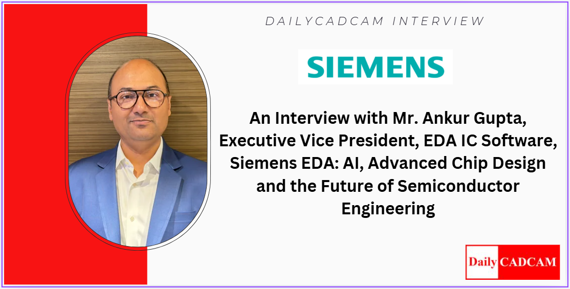
During Realize LIVE 2026 APAC in Bengaluru, DailyCADCAM Founder and Editor Mr. Sachin Nalawade spoke with Mr. Ankur Gupta, Executive Vice President, EDA IC Software at Siemens, about these developments and the future of semiconductor engineering.
Gupta brings more than two decades of experience across the EDA and simulation industries, having worked with Siemens, Ansys, and Cadence. In this conversation, he discusses the latest trends in chip and IC design, Siemens EDA’s technology portfolio, its collaboration with NVIDIA, recent acquisitions, digital twins, India’s growing semiconductor ecosystem, and the skills engineers and startups need for the future.
Q: Could you tell us more about your professional journey and your current role at Siemens?
Ankur Gupta: Let me give you the background in reverse chronological order.
At present, I am responsible for EDA IC Software at Siemens, and I have been with Siemens for about four years. I initially joined Siemens as the General Manager of our test product line, which is a market-leading product line.
Before Siemens, I spent about five years at Ansys. Ansys has a broad portfolio of simulation products, including solutions used for IC, package, and board applications.
Prior to Ansys, I spent a long period at Cadence, where I worked for approximately 16 years.
So, I have spent a significant part of my professional career in the EDA and simulation industries, looking at semiconductor design, verification, simulation, and related engineering workflows.
I grew up in India. I completed my bachelor’s degree at NIT Trichy and then pursued my master’s degree at Iowa State University in the US.
That is my professional background in a nutshell, and today my focus is on the IC software business within Siemens EDA.
Q: What are the latest trends you are seeing in chip design and IC design?
Ankur Gupta: One of the best ways to understand the trends is to look at the semiconductor market and understand what is driving its growth.
A lot of analysts are projecting that the semiconductor industry could grow to somewhere between $1.4 trillion and $2 trillion by 2030. The projection continues to change. Initially, people were talking about a trillion-dollar semiconductor industry by 2030, and now the estimates have increased significantly.
So, the important question is: what is driving this growth?
There are several major trends.
AI is driving demand for compute
The first major trend is artificial intelligence.
AI requires compute, and the demand for compute is growing much faster than the available supply. We are already hearing about shortages in areas such as memory and GPUs.
This means the semiconductor industry needs to build significantly more computing capability.
Moore’s Law is running out of steam
The second trend is related to semiconductor scaling.
You cannot simply keep putting more and more transistors into the same physical area anymore. Moore’s Law is running out of steam, and that is forcing the industry to look at new approaches.
One of those approaches is 3D semiconductor design.
New types of physics come into the picture when you move toward 2.5D and 3D architectures. There are significant interactions between thermal effects and mechanical stress, particularly because of thermal hotspots.
Silicon is no longer simply a 2D device.
We already have 2.5D architectures, where memory can be stacked alongside or integrated with logic. With 3D, we are moving toward logic stacked on logic.
You can almost think of it as a virtual skyscraper of silicon.
That creates enormous opportunities, but it also creates significant engineering challenges.
AI is also changing the chip-design process
The third major trend is that the entire design process needs to become more AI-powered.
Today, designing a chip can take 18 to 24 months. The industry is asking whether that can be reduced to nine months or perhaps 12 months.
So the question is: How do we reduce the time required to get to silicon?
AI has an important role to play in helping engineers explore more alternatives, automate repetitive work, and accelerate parts of the design process.
Software workloads are driving custom silicon
The fourth trend is the increasing use of custom or bespoke silicon.
The software workload increasingly determines what kind of hardware should be designed.
For example, you might have silicon specifically optimized for an AI training workload or AI inference workload. You could go further and design silicon optimized for processing text, images, or video.
Google’s Tensor Processing Unit (TPU) is a good example. Google looked at the software workload its hardware needed to run and developed a specialized accelerator instead of relying only on a generic accelerator such as a GPU.
So, these are some of the major trends shaping the semiconductor industry today.
Q: When it comes to design, simulation, testing, and verification, what solutions does Siemens offer, and how are they integrated with other Siemens platforms?
Ankur Gupta: I would divide this into two areas: first, the EDA-to-EDA portfolio, and second, how the EDA portfolio connects with the broader Siemens ecosystem.
If we look at the EDA portfolio, Siemens EDA has several market-leading products across the semiconductor design, verification, test, and manufacturing flow.
We are number one in test, and we are number one in physical verification with our Calibre product line.
We are also number one in high-sigma characterization of libraries with our Solido product line.
In the board design and analysis space, we have the Xpedition product line.
Beyond these established market-leading products, we have been investing significantly over the past several years in our analog mixed-signal platform.
On the digital side, we have also been building out our design platform. Historically, Mentor Graphics and Siemens EDA did not have a comprehensive design platform in this area, but now we have Aprisa, which provides physical design capabilities for modern SoC design.
We also have Analog FastSPICE, which supports verification for analog, RF, mixed-signal, and custom digital circuits.
For high-level synthesis, we have Catapult, which enables design teams to work with languages such as C++ and SystemC and implement those algorithms in IC designs.
We also have products such as PowerPro for power optimization and Empower for power-grid analysis.
On the hardware side, we have the Veloce platform for hardware/software and system validation.
For IC functional verification, we have the Questa platform, which supports functional verification and debugging of complex SoCs and FPGAs.
So, if you look at the complete EDA flow, we have capabilities across design, verification, test, physical verification, and related areas.
Some of these products are market-leading, while others are areas where we are continuing to invest and build competitive capabilities.
Connecting EDA with Siemens
Then you move beyond EDA into the broader Siemens portfolio.
The first domain is the chip or IC domain. Then you move into packaging and board design, where Xpedition plays an important role.
For 2.5D and 3D IC and advanced packaging, we have technologies such as Innovator3D IC and CloudBank.
These technologies address workflows involving heterogeneous integration of semiconductors.
Then you move into simulation. It is no longer just about simulation inside the chip. You need to consider package simulation, board simulation, thermal behavior, and eventually the complete system. That is where the Simcenter platform comes in.
And the connection does not stop at electronics.For example, imagine analyzing the thermal behavior of a chip or a blade inside a data center. EDA tools can generate information about the thermal characteristics, which can then be connected to Simcenter for broader thermal simulation.
That information can then reach the mechanical engineer working in Designcenter, who is designing the enclosure and determining where to position the heat sink.
Ultimately, even the software engineer can become part of that workflow because the cooling strategy can be influenced by the heat generated by the chip.
Some of these connections already exist, while others represent our broader vision of connecting these disciplines into a comprehensive digital twin.
Q: Siemens recently announced a collaboration with NVIDIA. What exactly is this collaboration about?
Ankur Gupta: We announced a total of four programs with NVIDIA. One of those programs focuses on AI-native EDA, while another focuses on simulation.
NVIDIA has GPUs, but it also has a broader software and AI ecosystem, including the CUDA-X software stack, Nemotron models, agentic frameworks such as NeMo Gym, and technologies such as OpenShell.
One important area of collaboration is helping Siemens engineers accelerate our algorithms. Our EDA algorithms are heavily based on computer science and mathematics. NVIDIA can provide expertise in identifying areas where those algorithms can be accelerated on GPUs. The goal is to help us complete that work faster.
The second important area is our Fuse EDA AI system.
Fuse is our generative AI and agentic AI system for semiconductor and PCB design. It is designed to bring AI capabilities into the EDA workflow while maintaining enterprise-level security and providing integration across the Siemens EDA portfolio. Fuse can connect with NVIDIA technologies such as Nemotron, NeMo Gym, and OpenShell.
Another important aspect is that Fuse is designed to be open to the industry. Customers may use different EDA vendors’ tools as part of their workflows. We are not trying to create an isolated environment. NVIDIA is also taking an open approach, so the combination of Siemens EDA and NVIDIA’s AI capabilities can provide significant benefits to semiconductor customers.
Q: Does Siemens EDA offer something similar to PLM for chip design, as we see in the mechanical industry?
Ankur Gupta: Siemens EDA provides a comprehensive software portfolio covering not just design but also design, verification, testing, and physical verification.
The semiconductor design process has its own unique requirements, and EDA tools address those requirements throughout the IC development and verification lifecycle. The important thing is to connect these capabilities so that engineers can move efficiently through the different stages of semiconductor development.
Q: Do you have digital twins in chip design and semiconductor engineering?
Ankur Gupta: Digital twins are somewhat different in EDA because the entire semiconductor design process is already digital. Consider a designer who wants to design a GPU. The process starts with a specification. That specification is digital. Then the design moves into a format such as RTL, where the functional behavior of the design is described digitally. From there, the design gradually moves toward formats such as GDS, where the physical implementation remains digital.
It is similar in concept to using CAD software to digitally design a building. The difference is that, in semiconductor engineering, the digital design eventually goes to a fabrication facility and becomes a physical chip. So, in our case, the process effectively starts digitally and then becomes real.
That is why semiconductor engineering has been operating in a digital-twin-like environment for a long time.
Q: Siemens recently announced acquisitions of Precision Innovations and Defacto Technologies. What do these companies bring to Siemens EDA?
Ankur Gupta: We recently announced two acquisitions: Precision Innovations, which is based in the US, and Defacto Technologies, which is based in France.
Precision Innovations brings together EDA capabilities and AI capabilities.
Its customers use its technology for areas such as estimation and auto-tuning.
One of the particularly interesting capabilities is early estimation of power, performance, and area, or PPA.
Imagine a chip architect who is evaluating different architectures.
They might ask: What would happen if I designed the chip this way? What would happen if I changed the architecture or macro placement?
Precision Innovations’ technology can estimate the PPA results for those different options. The designer can perform an A-B comparison, make a change, run another estimate, and understand how the PPA is changing. This is particularly valuable because today’s chip designers want to perform many experiments.
The industry increasingly wants machines to perform those experiments and provide engineers with information much earlier in the design process.
That is what makes this technology powerful.
Defacto Technologies
Defacto Technologies also plays an important role in SoC architecture and SoC planning.Its technologies support automation and continuity from design creation through implementation and have capabilities focused on areas such as low-power design. So, we are very excited about both acquisitions.
Excellicon
About six months earlier, Siemens also acquired Excellicon.
Excellicon brought software for the development, verification, and management of timing constraints into Siemens EDA’s IC design portfolio.The objective is to help SoC designers improve PPA, accelerate design closure, improve constraint correctness, increase productivity, and address gaps in existing workflows.
The combination of these acquisitions helps us build out the design and verification platform more robustly.
Q: When it comes to semiconductor manufacturing, does Siemens EDA work with the machines and special-purpose equipment used in fabs?
Ankur Gupta: Semiconductor manufacturing happens in fabs, or fabrication facilities. There are large fabs operated by companies such as TSMC, Samsung, and Intel. These facilities use highly specialized equipment, and companies such as ASML are major manufacturers of semiconductor manufacturing machines.
Our role as an EDA company is different. We help semiconductor companies design the chips. The completed digital design is then sent to the fab. The fab performs thousands of manufacturing steps to transform the silicon and create the different layers of the chip. Those processes include extremely complex operations such as etching, polishing, and building multiple layers.
So, semiconductor manufacturing is fundamentally different from mechanical manufacturing, where CAD and CAM systems can be closely connected to CNC machines and other manufacturing equipment.
Q: How do you see India as a market and as a semiconductor industry?
Ankur Gupta: India is already a very significant semiconductor design hub.
If you look at multinational companies operating in India as well as Indian-owned companies, my estimate is that somewhere around 35–40% of the worldwide chip designer population is in India. That represents a very strong user base. Chip design has been taking place in India for approximately 25–30 years, so this is not a completely new industry for the country.
What is changing now is that India is also beginning to see significant investment in semiconductor manufacturing and OSAT—outsourced semiconductor assembly and test. Starting a semiconductor fab is extremely complex. It requires deep investment, but capital is only one part of the challenge. You need a highly skilled workforce, reliable power, a reliable water supply, and extremely controlled environmental conditions. Even factors such as temperature, dust, and airborne particles become critical.
A semiconductor fab needs to maintain an environment with extremely low levels of contamination because very small particles can affect the manufacturing process. That is why building a new fab is difficult even for highly experienced semiconductor manufacturers.
TSMC, for example, has a well-established process for creating new fabs, but even for an experienced manufacturer, establishing a fab in a new geographic location is a major undertaking.
I believe the combination of government support and investment from an established company such as Tata provides an appropriate foundation for India to begin developing its semiconductor manufacturing capabilities. The collaboration of Tata Electronics with Taiwan-based Powerchip Semiconductor Manufacturing Corp. also makes sense because Taiwan has significant semiconductor manufacturing expertise.
Q: What would be your message to electronics and semiconductor engineers in India? What skills should they develop for the future?
Ankur Gupta: I would say that there is nothing better than personal experience when talking about this.
My own education was in electrical and electronics engineering, followed by VLSI, and my background combines computer science, computer architecture, and physics. Semiconductor engineering is complex. It is difficult. But it can also be an extremely rewarding career.
My message to students in India would be to focus very strongly on building their fundamentals during their bachelor’s and master’s education. The more complex the subject you learn, the stronger your ability becomes to solve challenging engineering problems. That foundation becomes particularly important as technology evolves.
We are moving into an AI-driven world, but AI does not eliminate the need to understand semiconductor physics. There will always be a need to model semiconductor behavior and develop algorithms that are heavily based on computer science, mathematics, and engineering principles.
AI will provide another layer that helps engineers perform that work more efficiently.
So, my recommendation is to build strong fundamentals in areas such as computer engineering and computer science, along with the electronics, mathematics, physics, and architecture knowledge needed for semiconductor engineering.
Q: How can students and existing users learn Siemens EDA software and advanced semiconductor design technologies? Does Siemens provide online education or training?
Ankur Gupta: Yes. Siemens has a strong educational program.
For students and incoming users who want to learn Siemens software, we work with universities in India, and there is an opportunity to expand these programs further.
For engineers who are already employed in companies using Siemens software, we have educational credits. If a company owns Siemens software, those credits can be used to continue training junior engineers and help them develop their skills.
We also have startup programs.
Startups often do not have the financial resources of large semiconductor companies, so purchasing EDA software can be a significant challenge. Our startup programs are intended to make the software available to startups at a more reasonable cost.
So the objective is to support the entire ecosystem—from students and early-career engineers to established users, startups, and large enterprises.
Q: What would be your message to semiconductor startups in India?
Ankur Gupta: I think there is a significant opportunity for semiconductor startups in India.
This is also a topic that has come up in discussions involving the Government of India, ministers, educators, and large multinational semiconductor companies. India has major multinational companies employing thousands and sometimes tens of thousands of engineers. There is an opportunity for these large organizations to encourage experienced engineers and leaders to become entrepreneurs and start new companies. The larger companies can also play a role in supporting these startups.
From the EDA startup perspective, Siemens EDA has a collaboration program called Open Door. Through Open Door, we can help EDA startups access Siemens software. For a startup, access to EDA software can be a major barrier. If engineers have a good idea but cannot access the necessary tools, it becomes difficult to develop and validate that idea. Programs such as Open Door are intended to help remove that barrier and encourage innovation in the EDA ecosystem.
A sincere thank you to Mr. Ankur Gupta, Executive Vice President, EDA IC Software at Siemens, for taking the time to speak with DailyCADCAM Editor Sachin Nalawade during Realize LIVE 2026 APAC in Bengaluru.
It was a pleasure discussing the rapidly evolving semiconductor and electronics industry, including AI-driven EDA, advanced 2.5D/3D chip design, simulation, verification, digital twins, and the growing semiconductor ecosystem in India.
Your insights on the future of semiconductor engineering, the role of AI, and the opportunities for engineers and startups in India will be valuable to DailyCADCAM readers across electronics, semiconductor, and EDA communities.
Thank you once again for sharing your time, expertise, and vision with DailyCADCAM. We truly appreciate the opportunity to bring this conversation to our readers.